
Chapter 12
PROPERTIES OF OBJECTS
Properties of various objects are edited in the Properties dialog box and the Objects tab of the Side Panel.
12.1 Properties Dialog Box
To open the Properties dialog box, press the [Properties] button in the Style tab of the Side Panel. The same dialog box can be open by choosing one of submenus in the “Objects” menu \(\Rightarrow \) “Properties”. When “Preview” is checked, changes in the Properties dialog box are reflected on the Graphics Area in real time. Click [OK] to apply all the changes or [cancel] to discard the changes. Current properties are saved as default values in VESTA by clicking the [Save as default] button.
12.1.1 General
The first page in the Properties dialog box is General (Fig. 12.1).
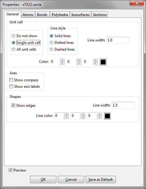
Unit cell
The display of Unit cell edges in the Graphics Area is controlled with the following three radio buttons:
- “Do not show”: Do not show unit cell edges.
- “Single unit cell”: Show edges of a single unit cell.
- “All unit cells”: Show all the edges of unit cells within the drawing boundary.
Line styles of the unit cell edges are selected from three styles: “Solid lines”, “Dotted lines”, and “Dashed lines”. The width of lines is input in text box {Line width}. The color of lines is specified either (A) by entering R, G, and B values ranging from 0 to 255 or (B) by picking a color from a color selection dialog box opened after clicking the [Select] button.
Axes
“Show Compass” is used to turn on or off a display of three arrows indicating \(a\), \(b\), and \(c\) axes (or \(x\), \(y\), and \(z\) axes in the case of Cartesian coordinates). “Show Axis Labels” is used to turn on or off a display of axis labels, ‘a’, ‘b’, and ‘c’ (or ‘x’, ‘y’, and ‘z’ in the case of Cartesian coordinates).
Shapes
The visibility, line width, and color of edges of crystal morphologies are input in the Shapes frame box.
12.1.2 Atoms
The second page in the Properties dialog box is Atoms (Fig. 12.2).
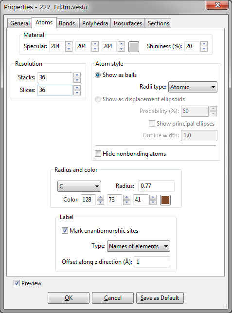
Material
- {Specular} is a color of reflected light that bounces sharply in a particular direction in the manner of a mirror. A highly specular light tends to cause a bright spot on the surface it shines upon, which is called the specular highlight.
- {Shininess} is a property, which specifies how small and focused the specular highlight. A value of 0 specifies an unfocused specular highlight.
Resolution
{Stacks} and {Slices} are parameters common to all the atoms, allowing you to change the resolution (quality) of atoms displayed on the screen. {Stacks} denotes the numbers of subdivisions along the \(Z\) axis (similar to lines of latitude) while {Slices} denotes the number of subdivisions around the \(Z\) axis (similar to lines of longitude). {Stacks} and {Slices} should be equal to each other in ball-and-stick and space-filling models where atoms are represented by perfect spheres. In general, decreasing {Stacks} and {Slices} accelerates the rendering of objects in the Graphics Area.
Atom style
Select either of the following two radio buttons for the mode of displaying atoms on the Graphics Area: (1) “Show as balls” or (2) “Show as displacement ellipsoids”.
- “Show as balls”: Atoms are rendered as spheres. List box {Radii type} is used to select a type of default atomic radii from the following three:
- Atomic: Metallic or covalent radii, whose values were mostly taken from Refs. [74, 75, 76].
- Ionic: Effective ionic radii compiled by Shannon [77] for representative oxidation states and coordination numbers.
- van der Waals: van der Waals radii [78].
The user may modify default values of atomic, ionic, and van der Waals radii by editing a text file, elements.ini, in the program folder of VESTA.
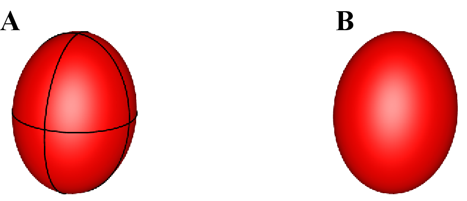
- “Show as displacement ellipsoids”: Atoms are rendered as ellipsoids to represent anisotropic displacement of atoms whose shapes are calculated from anisotropic atomic displacement parameters, \(\beta _{ij}\) or \(U_{ij}\) (see 6.3.5). The probability (in percentage) for atomic nuclei to be included in the ellipsoids is input in text box {Probability}. It is common to all the atoms when drawing displacement ellipsoids. If option “Show principal ellipses” is checked, three principal ellipses corresponding to three principal planes are plotted on the surface of each ellipsoid (Fig. 12.3). The line width of the principal ellipses is input in text box {Line width}.
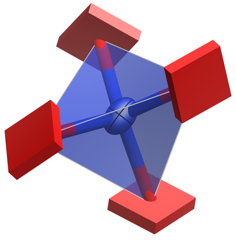
If one or more of principal axes have negative mean square displacements, atoms are represented by cuboids so that the unusual atomic displacement parameters can easily be recognized (Fig. 12.4). Each cuboid is oriented in accordance with principal axes with the dimension of the cuboid scaled according to the absolute value of the mean-square displacement.
- “Hide non-bonding atoms”: This option hides atoms that are connected by no bonds but the crystallographic site for those atoms have a coordination number larger than 0. In other words, atoms are made invisible if all the coordinated atoms are lying outside of the drawing boundary.
Radius and color
Select a symbol of an element from list box {Symbol} and then specify its {Radius}. The color of an atom (element) is specified either (a) by entering R, G, and B values ranging from 0 to 255 or (b) by picking a color from a color selection dialog box opened when clicking the [Select] button.
Labels
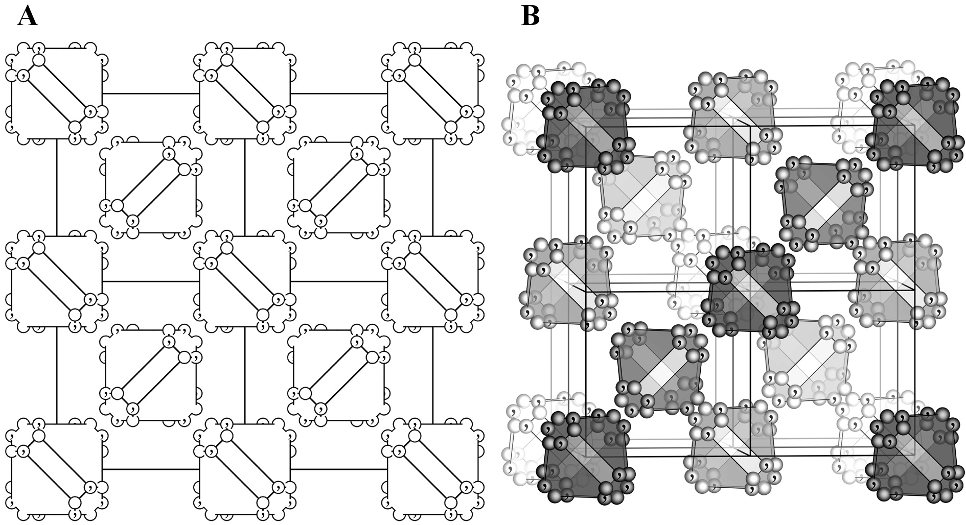
Select either of the following two types for atom labels: (1) “Names of elements” or (2) “Names of sites”. Labels are displayed near atoms with an offset along the \(z\) axis, which is specified in the unit of Å. When option “Mark enantiomorphic sites” is checked, atoms generated by symmetry operations of inversion, rotoinversion, or mirror are marked with a ‘,’ symbol. These positions are enantiomorphs with respect to non-marked positions. This option can be used to draw general position diagrams (Fig. 12.5) similar to those illustrated in “International Tables for Crystallography,” Vol. A [30]. When an atom position coincides with an a enantiomorphic symmetry element, the original and enantiomorphic positions coincide. Such an atom is represented by a ‘,’ mark on the left half of the atom separated with ‘\(\mid \)’ at its center.
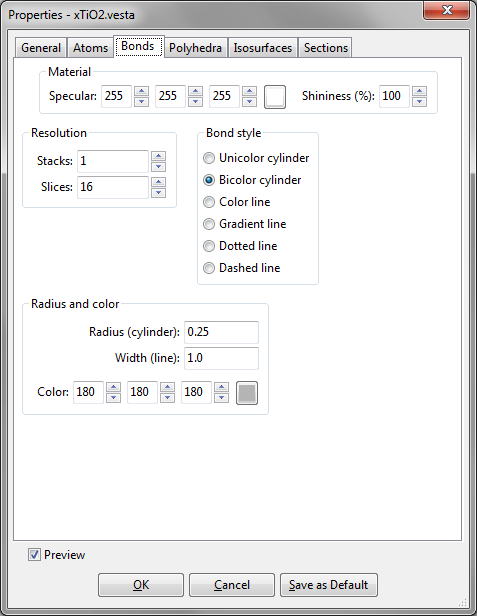
12.1.3 Bonds
The third page in the Properties dialog box is Bonds (Fig. 12.6).
Material
It is the same as that in Atoms (see 12.1.2).
Resolution
It is the same as that in Atoms (see 12.1.2).
Bond style
One of the following six types of bonds are specified in this frame box:
- “Unicolor cylinder”: Each bond is drawn as a cylinder, whose color can be changed in the Color panel.
- “Bicolor cylinder”: Each bond is drawn as a cylinder with colors of two atoms connected with each other. The two colors of the bond are just the same as those of atoms connected by bonds.
- “Color line”: Each bond is drawn as a straight line, whose color is changed in the Color panel.
- “Gradient line”: Each bond is drawn as a line connecting two atoms with gradient distribution of colors. Colors of each bond at the ends of the line are the same as those of the atoms.
- “Dotted line”
- “Dashed line”
Radius and color
The radius of each cylindrical bond in the stick model is changed in text box {Radius (cylinder)}. The actual radius of cylinders is 40 % of the input value. The line width of line-style bonds is changed in text box, {Width (line)}. The color of bonds in the single color style is changed in the Color tool below these two text boxes.
12.1.4 Polyhedra
The fourth page in the Properties dialog box is Polydedra (Fig. 12.7).
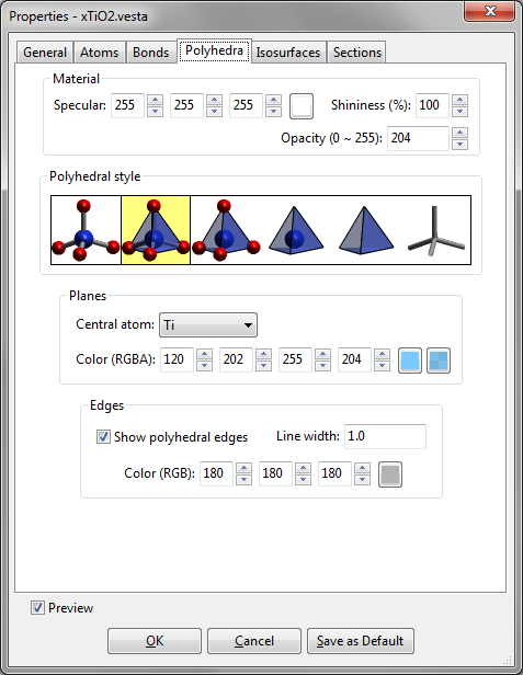
Material
{Specular} and {Shininess} are just the same as those in Atoms page (see 12.1.2). The {Opacity} of coordination polyhedra is input with 255 corresponding to opaque planes (the inside of each coordination polyhedron is invisible) and 0 corresponding to fully transparent planes (coordination polyhedra are invisible).
Polyhedral style
Styles of coordination polyhedra are selected from the following six types of expressions that are schematically illustrated in the Polyhedral style frame box:
- Show atoms and bonds without any coordination polyhedra.
- Show atoms, bonds, and coordination polyhedra (default).
- Show atoms and coordination polyhedra.
- Show central atoms and coordination polyhedra.
- Show only coordination polyhedra.
- Show only bonds.
Planes
The surface color of each coordination polyhedron is specified here. Select an element from list box {Central atom} to specify its color. Default colors of coordination polyhedra are the same as those of the central atoms.
Edges
The visibility, line width, and color of edges of coordination polyhedra are input in the Edges frame box.
12.1.5 Isosurfaces
The fifth page in the Properties dialog box is Isosurface (Fig. 12.8).
Material
It is the same as that in Atoms (see 12.1.2).
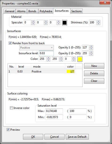
Isosurfaces
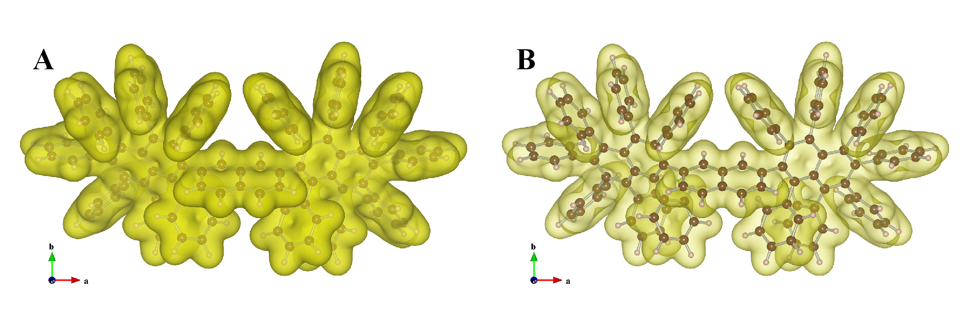
At the top of the Isosurfaces frame box, the minimum and maximum data values are displayed in the unit of the raw data. Data values such as electron and nuclear densities, and wave functions on isosurfaces are equal to {Isosurface level}, \(d\)(iso). All the points with densities larger than \(d\)(iso) lie inside the isosurfaces whereas those with densities smaller than \(d\)(iso) are situated outside the isosurfaces.
At the lower half of the frame box, a list of isosurface levels is shown. To add a new isosurface level, add the [New] button, and edit the isosurface level and color. To delete an isosurface level, select an item in the list, and press the [Delete] button. Pressing the [Clear] button deletes all the isosurfaces.
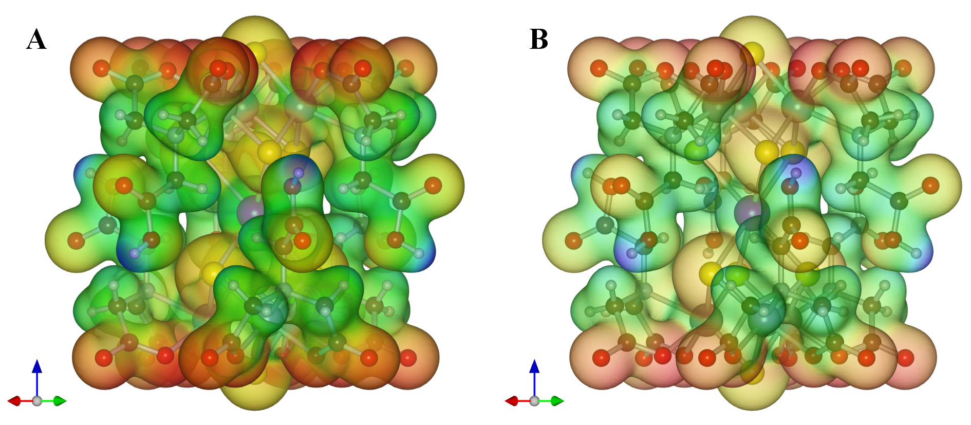
Order of rendering polygons The sequence of drawing polygons can be changed with option “Render from front to back.” By default, polygons are rendered from behind so that isosurfaces behind the nearest surface are visible through translucent isosurfaces. In some cases with complex isosurfaces, it may become difficult to understand the shape of isosurfaces because they heavily overlap each other. When option “Render from front to back” is checked, only the nearest surfaces are rendered. The use of this option may sometimes improve the visibility of complex isosurfaces because neither back surfaces nor internal ones are drawn.
Figure 12.9 illustrates a difference between the two rendering modes in 3D visualization of results of an electronic-state calculation for the [Cd{S\(_4\)Mo\(_3\)(Hnta)\(_3\)}\(_2\)]\(^{4-}\) ion (H\(_3\)nta: nitrilotriacetic acid) [79] by a discrete variational X\(\alpha \) method with DVSCAT [58].
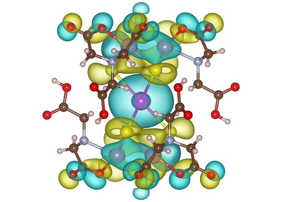
Kinds of isosurfaces For volumetric data having both positive and negative values, you can select which surfaces are visible:
- {Positive and negative},
- {Positive},
- {Negative}.
Figure 12.10 exemplifies isosurfaces of wave functions calculated with DVSCAT [58] for a complex ion with a ball-and-stick model superimposed on the isosurfaces. Yellow and blue surfaces show positive and negative values, respectively.
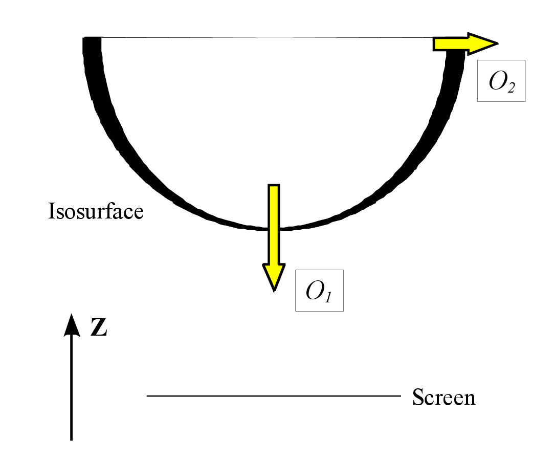
Opacity of isosurfaces The opacity of isosurfaces is specified by two parameters, {Opacity 1} (\(O_1\)) and {Opacity 2} (\(O_2\)), as exemplified in Fig. 12.11. \(O_1\) is the opacity for polygons parallel to the screen, and \(O_2\) is that for polygons perpendicular to the screen (Fig. 12.12). The opacity, O(\(p\)), for polygon \(p\) with a normal vector of (\(x\), \(y\), \(z\)) is calculated with a linear combination of \(O_1\) and \(O_2\):
Surface coloring
After volumetric data for surface coloring have been loaded, isosurfaces can be colored according to those data. The saturation level of colors is specified as (a) a value normalized between 0 and 100, and (b) a value corresponding to raw data. This is mostly equal to color settings for lattice planes and sections of isosurfaces (see 12.1.6), except that the normalized values of 0 and 100 corresponds to the minimum and maximum data values on the current isosurfaces, not the data set itself.
The color index, \(T\), to determine the color of a data point with a value of \(d\) is calculated from the unit of the raw data: the minimum saturation level, \(S_{\mathrm {min}}\), and the maximum one, \(S_{\mathrm {max}}\), in the unit of the raw data: \begin {equation} T = \frac {d - S_\mathrm {min}}{S_\mathrm {max} - S_\mathrm {min}} . \end {equation} Data points with values larger than \(S_{\mathrm {max}}\) and smaller than \(S_{\mathrm {min}}\) are given the same colors as those assigned to \(S_{\mathrm {min}}\) and \(S_{\mathrm {max}}\), respectively. \begin {equation} O_p = O_1 z + O_2 (1-z) . \end {equation}
12.1.6 Sections
The seventh (final) page in the Properties dialog box is Sections (Fig. 12.13).
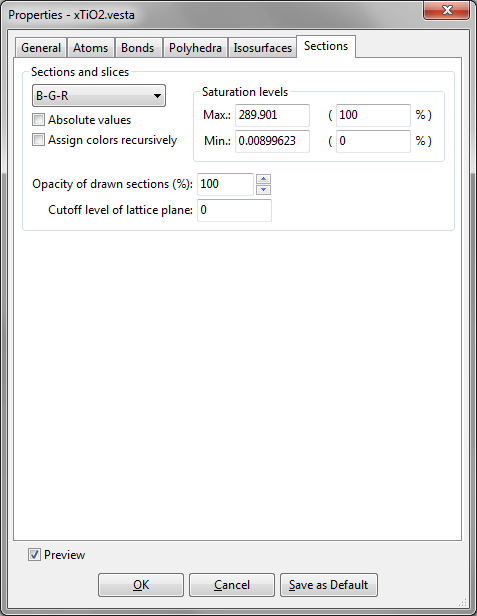
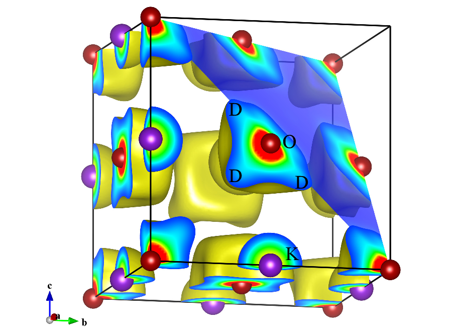
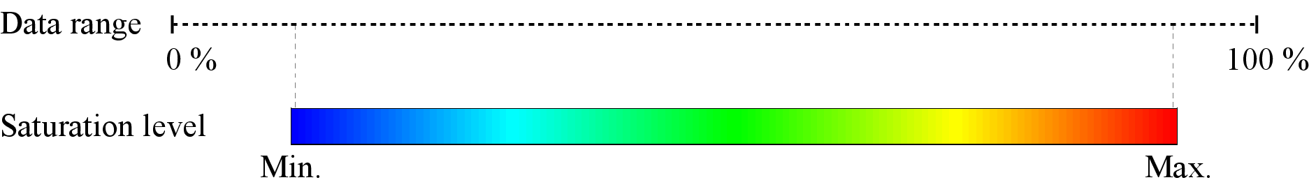
For volumetric data, both lattice planes and sections of isosurfaces are colored according to numerical values on them (Fig. 12.14). The saturation level of colors is specified as (a) a value normalized between 0 and 100 corresponding the minimum and maximum data values, respectively, and (b) a value corresponding to raw data. The color index, \(T\), for a data point with a value of \(d\) is calculated from the minimum saturation level, \(S_{\mathrm {min}}\), and the maximum one, \(S_{\mathrm {max}}\), in the unit of the raw data: \begin {equation} T = \frac {d - S_\mathrm {min}}{S_\mathrm {max} - S_\mathrm {min}} . \end {equation} Data points with numerical values larger than \(S_{\mathrm {max}}\) and smaller than \(S_{\mathrm {min}}\) are given the same colors as those assigned to \(S_{\mathrm {min}}\) and \(S_{\mathrm {max}}\), respectively. The color of each point is determined from \(T\), depending on color modes. One of six color modes, that is, B-G-R, R-G-B, C-M-Y, Y-M-C, gray scale (from black to white), and inverse gray scale, is selected from a list box. For example, blue is assigned to 0, green to 0.5, and red to 1 in the B-G-R mode, as shown in Fig. 12.15.
When option “Absolute values” is checked, colors are assigned on the basis of absolute values of data.
Option “Assign colors recursively” assigns rainbow colors recursively to data points with values smaller or larger than the saturation levels, which affords an effect similar to contour lines with gradient colors in between them. The opacity of sections are specified in the {Opacity of drawn sections} box, and that of lattice planes in the Lattice Planes dialog box (see 9.2). When {Cutoff level of lattice plane} is larger than 0, some parts of lattice planes with data values smaller than the cutoff level are omitted.
12.2 Objects Tab in the Side Panel
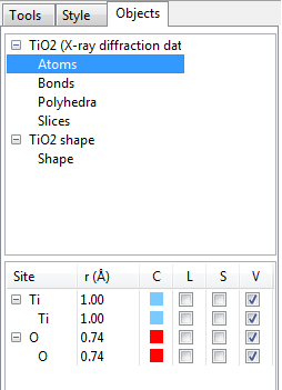
12.2.1 List of phases and objects
At the upper half of the Objects page, an overview of objects contained in each phase is listed (Fig. 12.16). Atoms, bonds, polyhedra, slices, and shapes are shown for each phase if they are contained in the phase data. Select one of them to see more details in objects at the lower half of the page.
12.2.2 Atoms
The first column (Site) lists crystallographic sites grouped by elements. The second column (r\(\,\)(Å)) gives radii for elements and crystallographic sites. To edit these data, select a row and click on the text. The third column (C) shows colors of atoms, which can be edited by double-clicking square areas. The fourth to sixth columns (L, S, and V) control visual properties of atoms, i.e., labels, selection states, and visibility. If properties of an element are edited, the modifications are applied to all the sites of the element.
12.2.3 Bonds
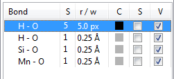
When a list of bond specifications is displayed in the lower half of the Objects page (Fig. 12.17), the first column (Bond) gives pairs of atoms that are bonded to each other. The second column (S) shows styles of bonds, which can be changed by double-clicking the second column of a bond. The third column (r/w) gives radii or line widths of bonds. When bonds are rendered as cylinders (styles 1 and 2), they are specified in the unit of Å, which are then rescaled by a factor of 0.4 on rendering of bonds. When bonds are rendered as solid, dashed, or dotted lines (styles 3–6), they are specified in the unit of pixels. The fourth column (C) displays colors of bonds, which are edited by double-clicking the colored square. The fifth and sixth columns (S and V) control selection states and visibilities of bonds, respectively.
12.2.4 Polyhedra
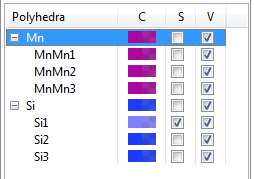
When a list of polyhedra is displayed in the lower half of the Objects page (Fig. 12.18), the first column (polyhedra) gives crystallographic sites grouped by elements. The second column (C) shows colors and opacities of polyhedra. The third and fourth columns (S and V) control selection states and visibilities of polyhedra, respectively. If polyhedral properties of an element are edited, the modifications are applied to all the sites of the element.
12.2.5 Slices
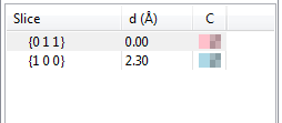
When a list of slices is displayed in the lower half of the Objects page (Fig. 12.19), the first column (Slice) gives Miller indices of slices. The second column (d\(\,\)(Å)) is distances from the origin to the slices, and the third column (C) shows colors and opacities of slices.
12.2.6 Shapes
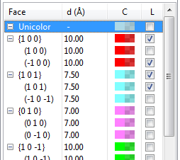
When a list of forms and faces of crystal morphologies is displayed in the lower half of the Objects page (Fig. 12.20), the first row is assigned to a special item to control a color of shape in the “Unicolor” style and the visibility of labels all at once. The first column (Face) gives Miller indices of faces grouped by crystallographically equivalent forms. The second column (d\(\,\)(Å)) is distances from the origin to faces, and the third one (C) shows colors and opacities of faces. The fourth column (L) controls the visibility of labels for faces. If properties of a form are edited, the modifications are applied to all the faces that are crystallographically equivalent.
